A selection of research and engineering projects from my professional and Ph.D. work.
Semiconductor Manufacturing & Process Development | Lux Semiconductors
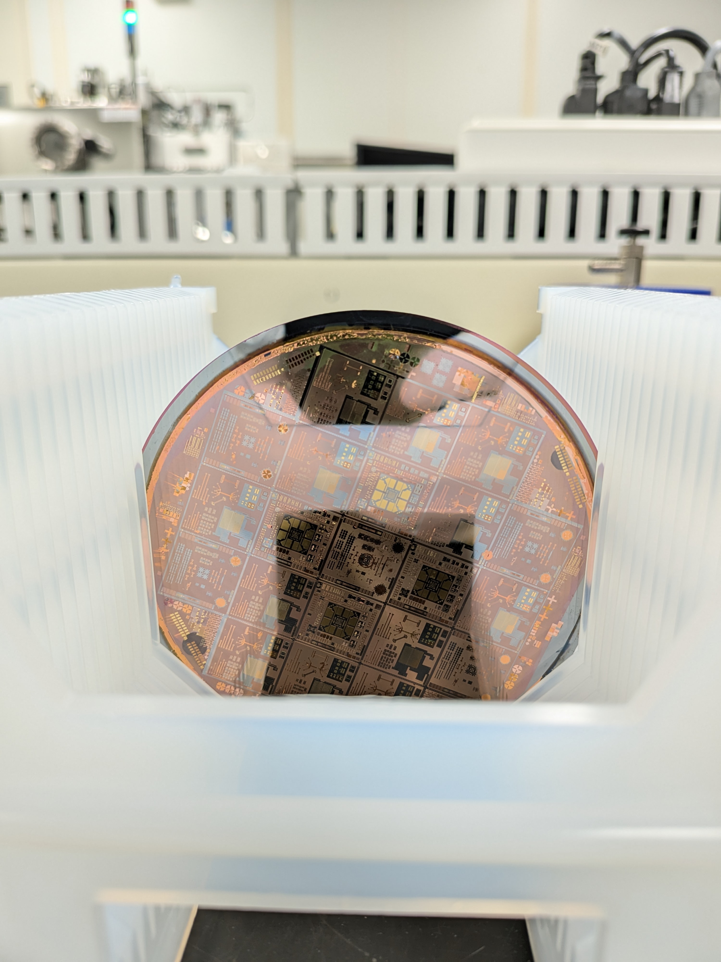
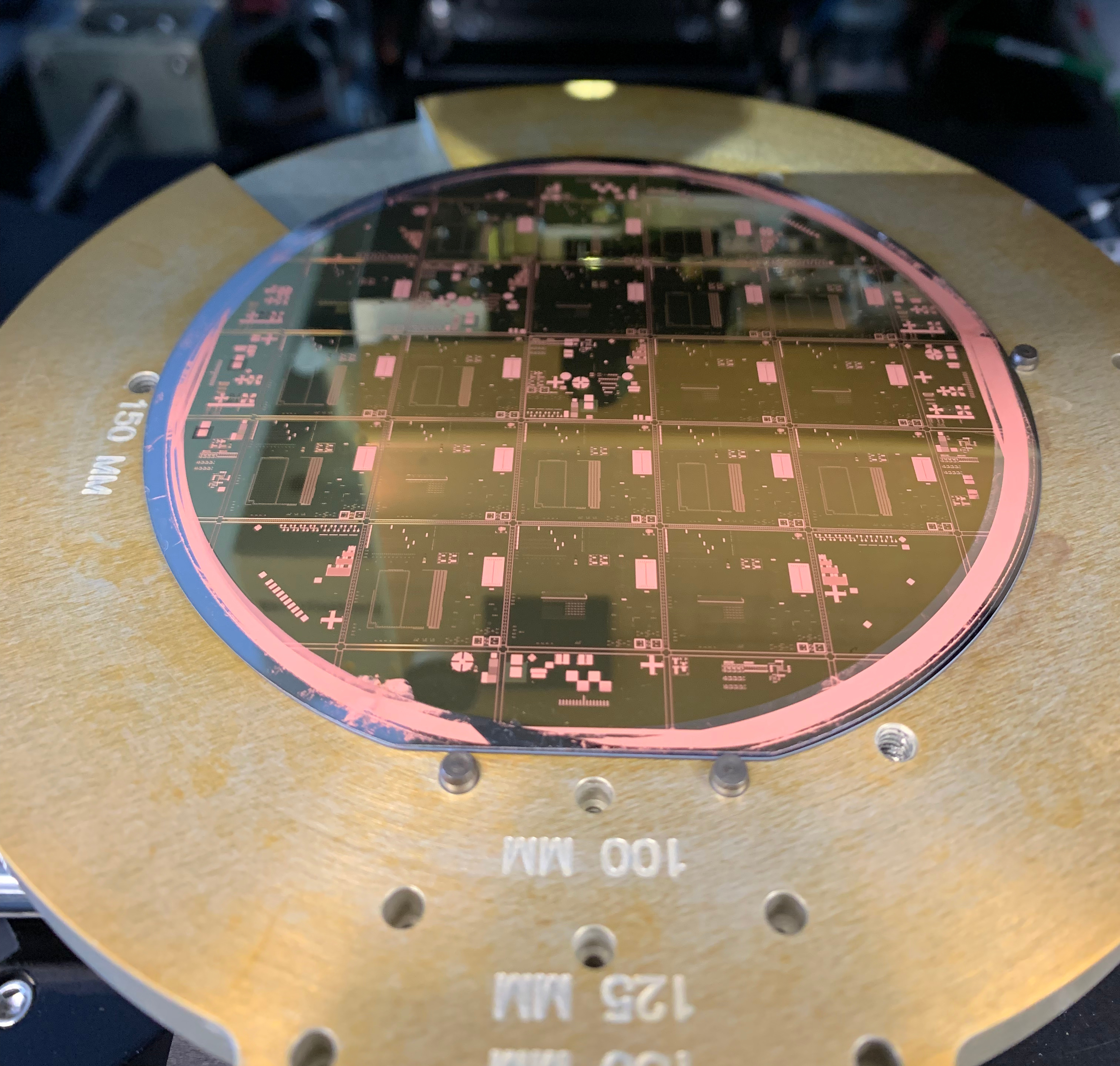
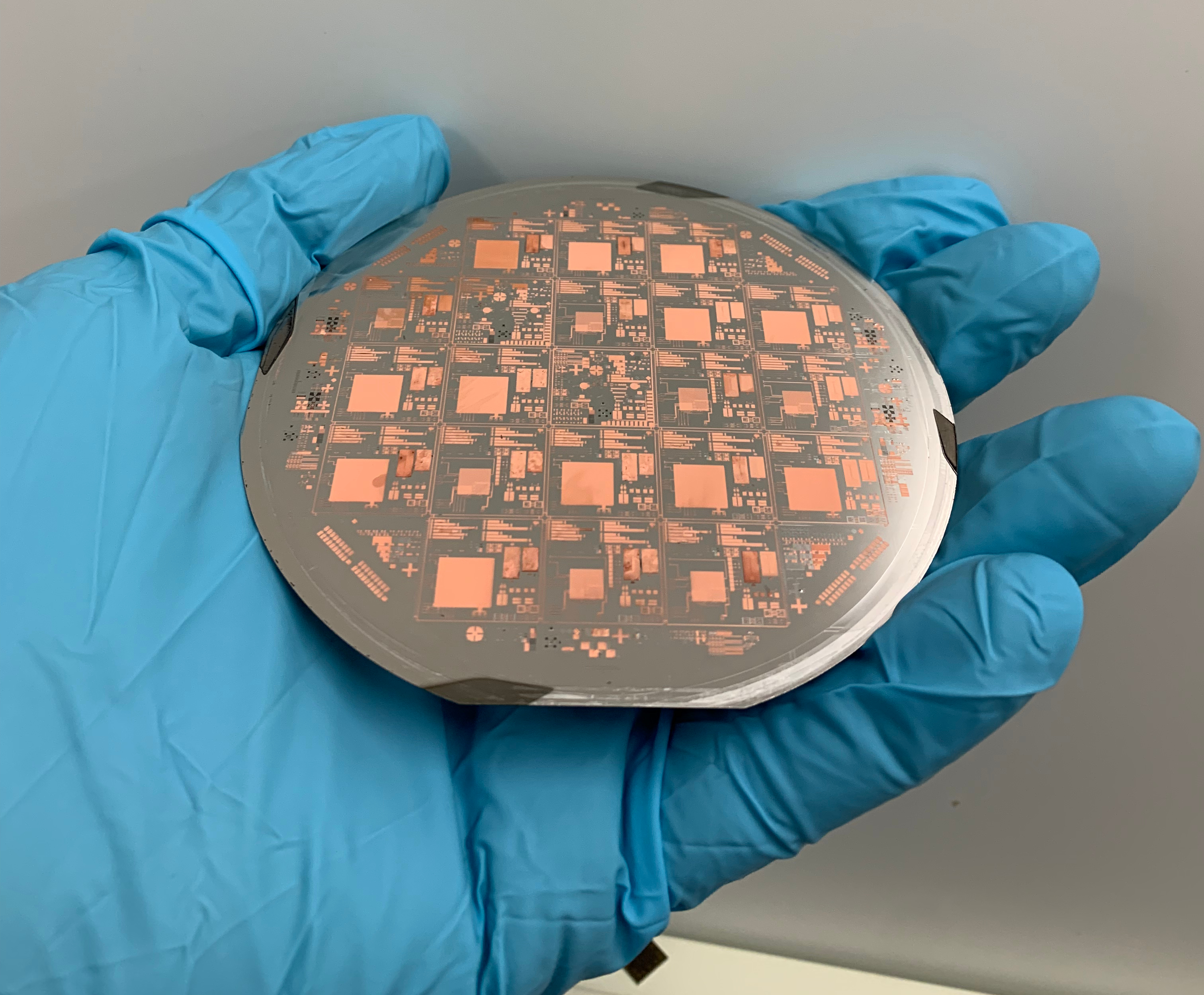
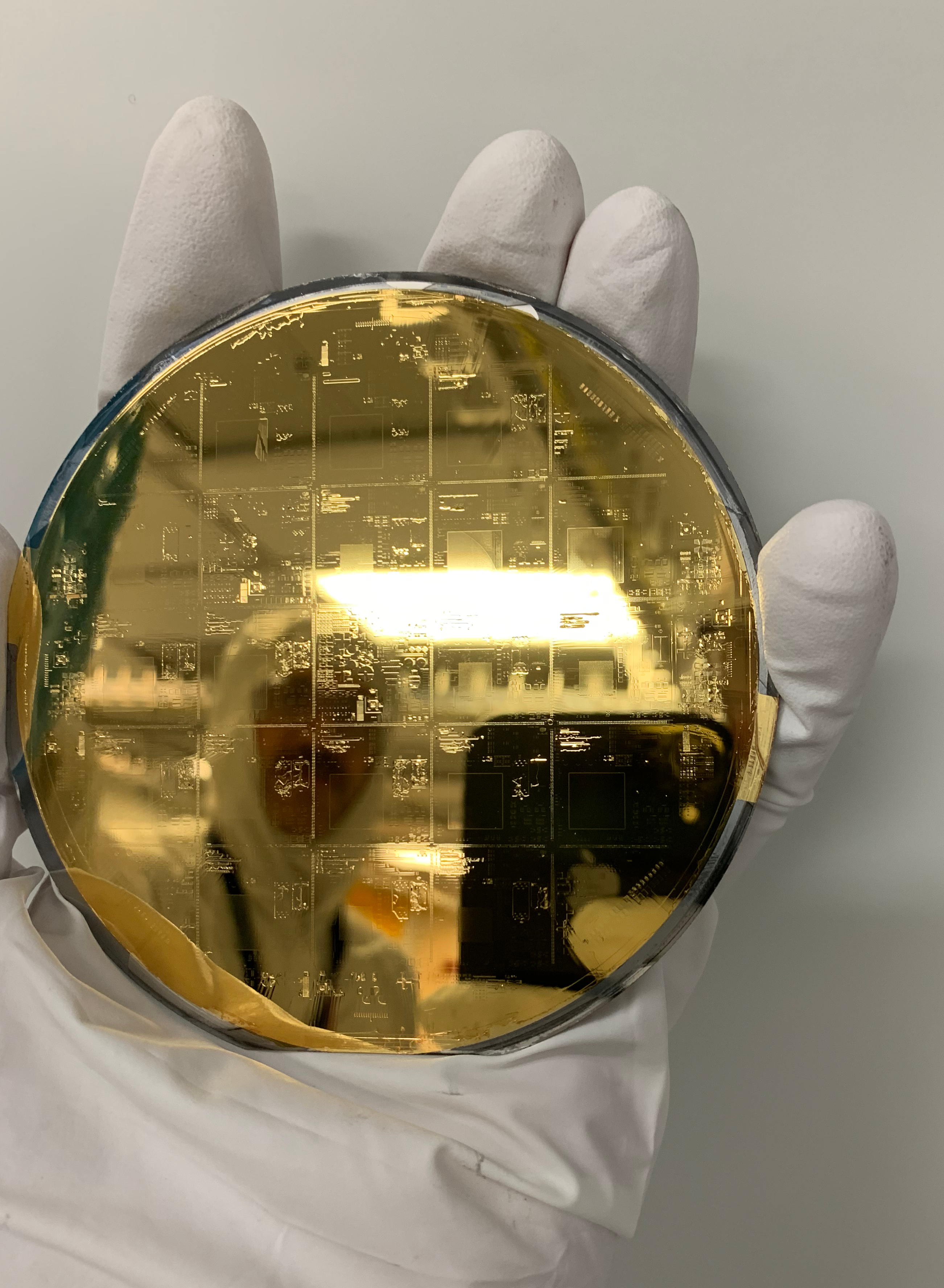
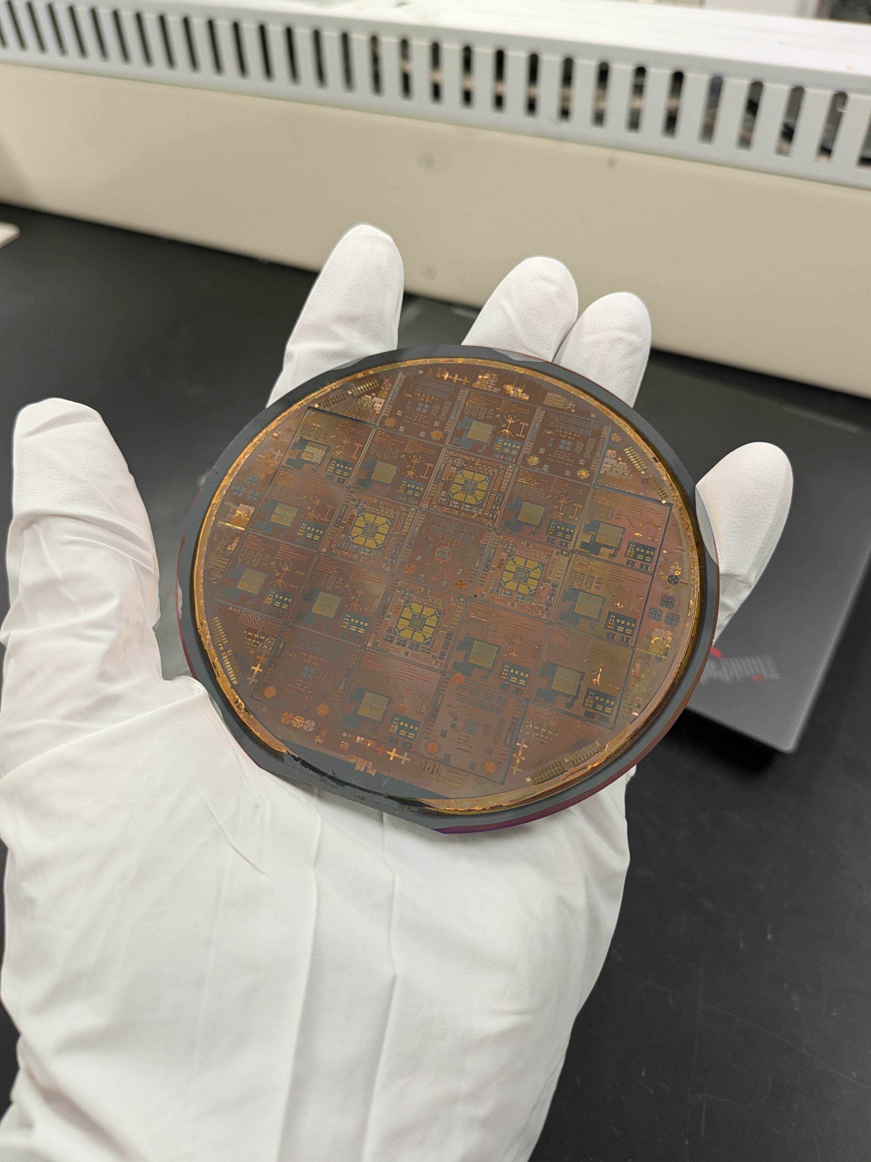
As an advanced packaging engineer at Lux, I thrived in a fast pace startup environment as a lead engineer. My experience spanned lab management, wafer fab, and through metal via formation for fan out wafer level and panel level packaging (FOWLP/FOPLP) on advanced metal substrates.
- Fabricated and optimized redistribution layers on metal wafers using a dual damascene process in the Cornell NanoScale Facility (CNF) for advanced interposer applications
- Managed a team to design and implement a novel process for fabricating through-metal-vias using femtosecond IR laser ablation
- Specializes in back end of line semiconductor fabrication techniques (plasma etching, sputtering, CVD, photolithography, electroplating)
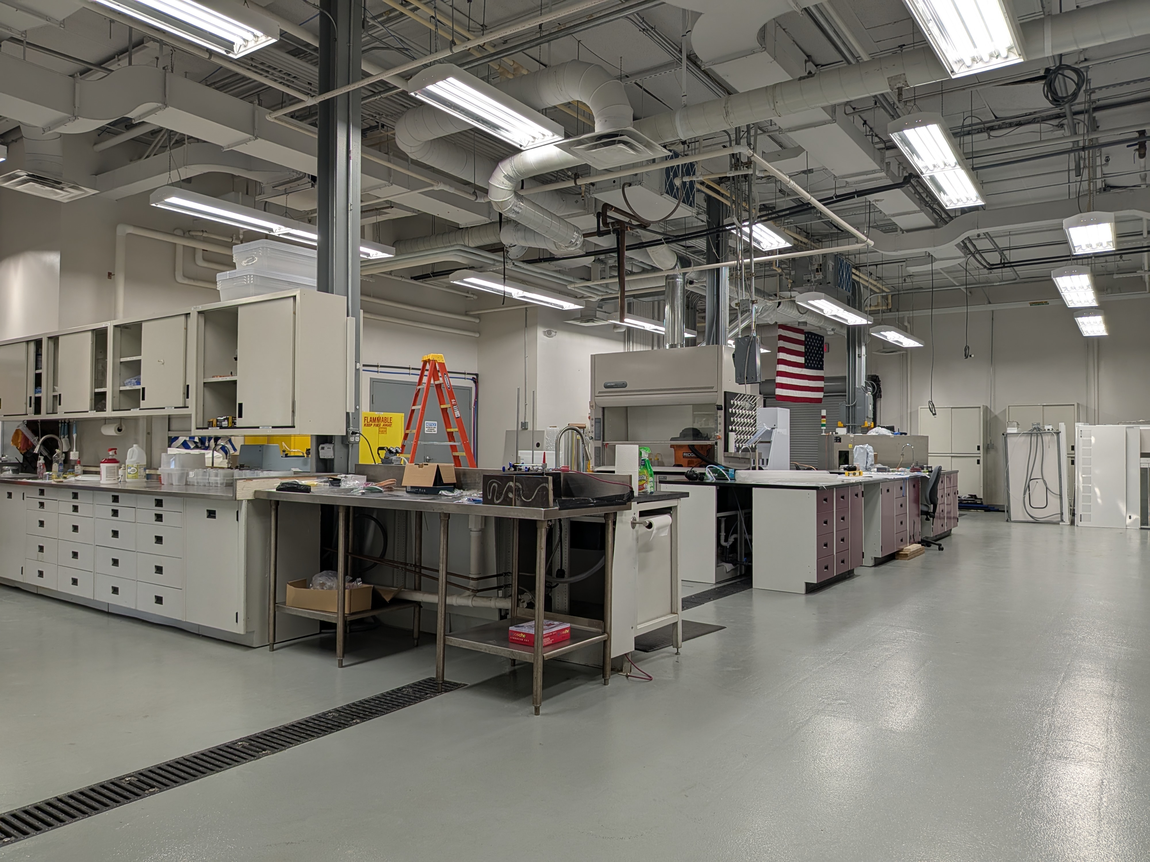
- Established a 6000 ft2 lab to develop Lux’s patented through-metal-via technology and deliver prototypes
Tech: Semiconductor processing, device fabrication, packaging, yield optimization
View details
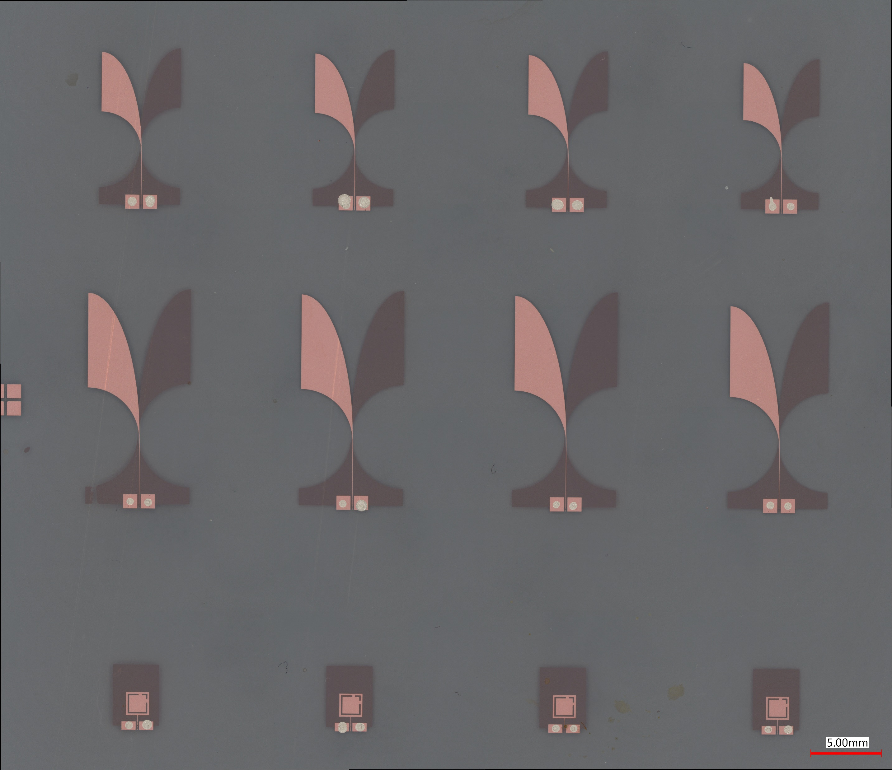
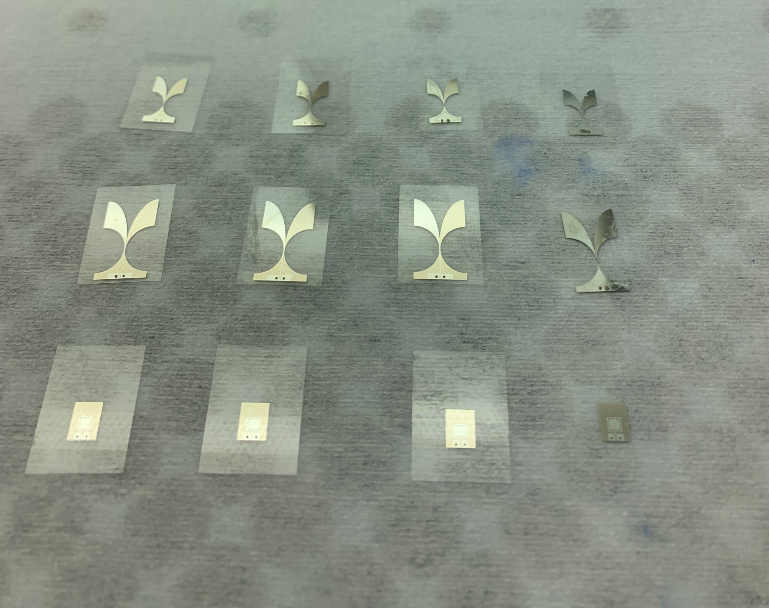
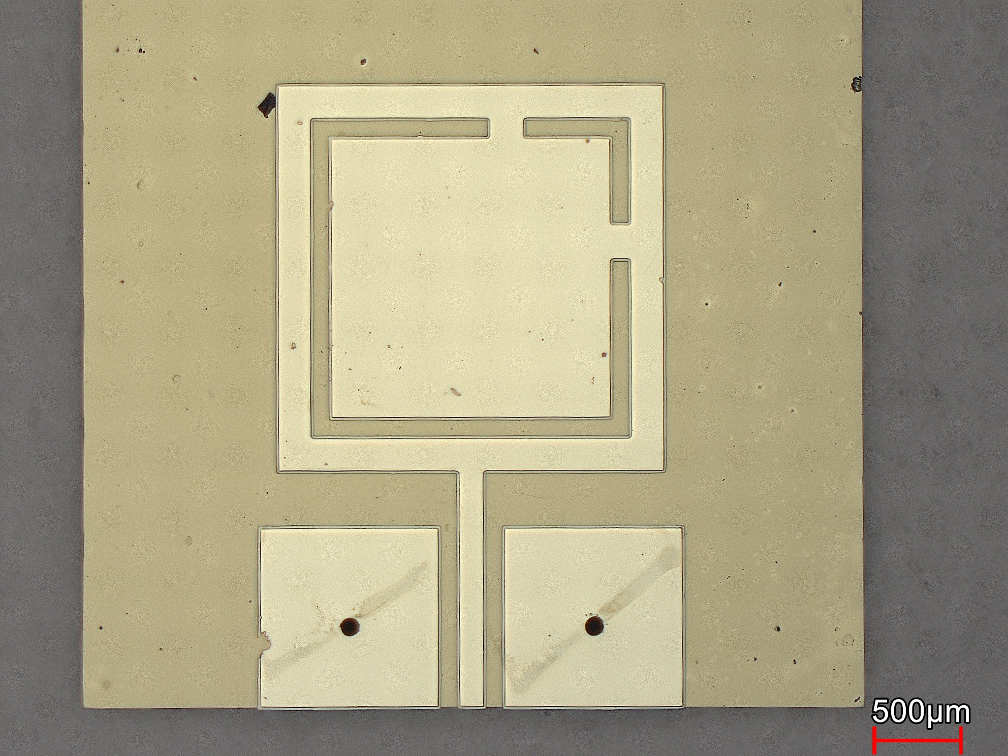
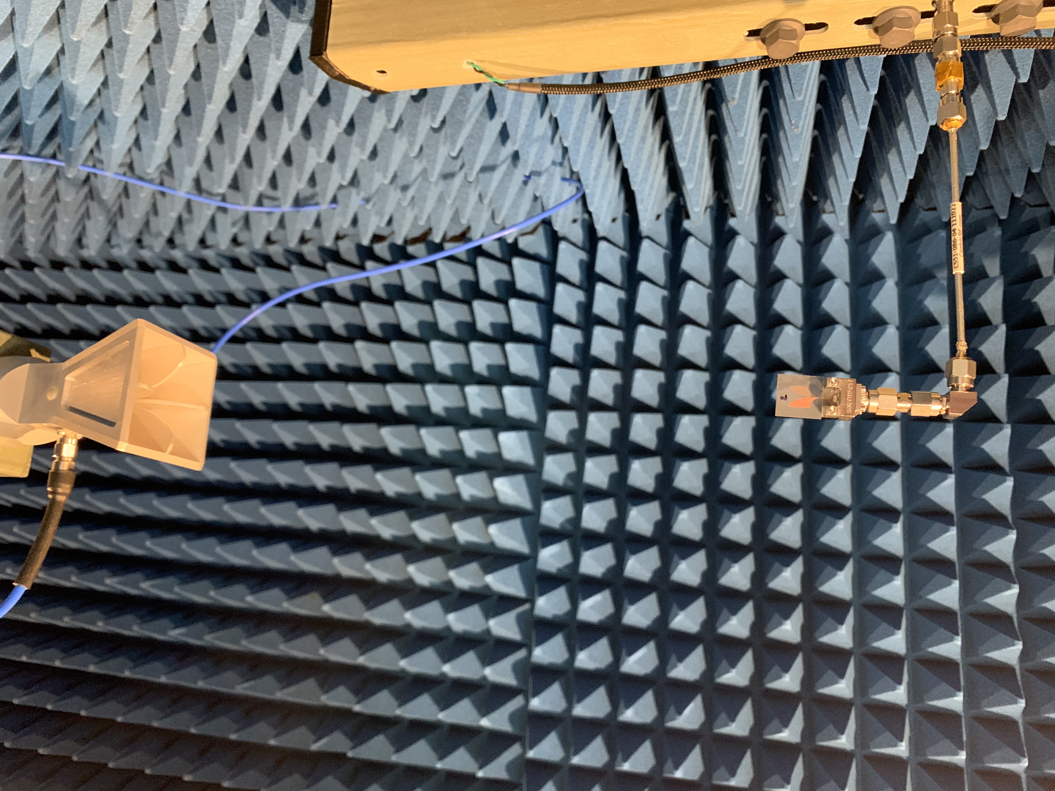
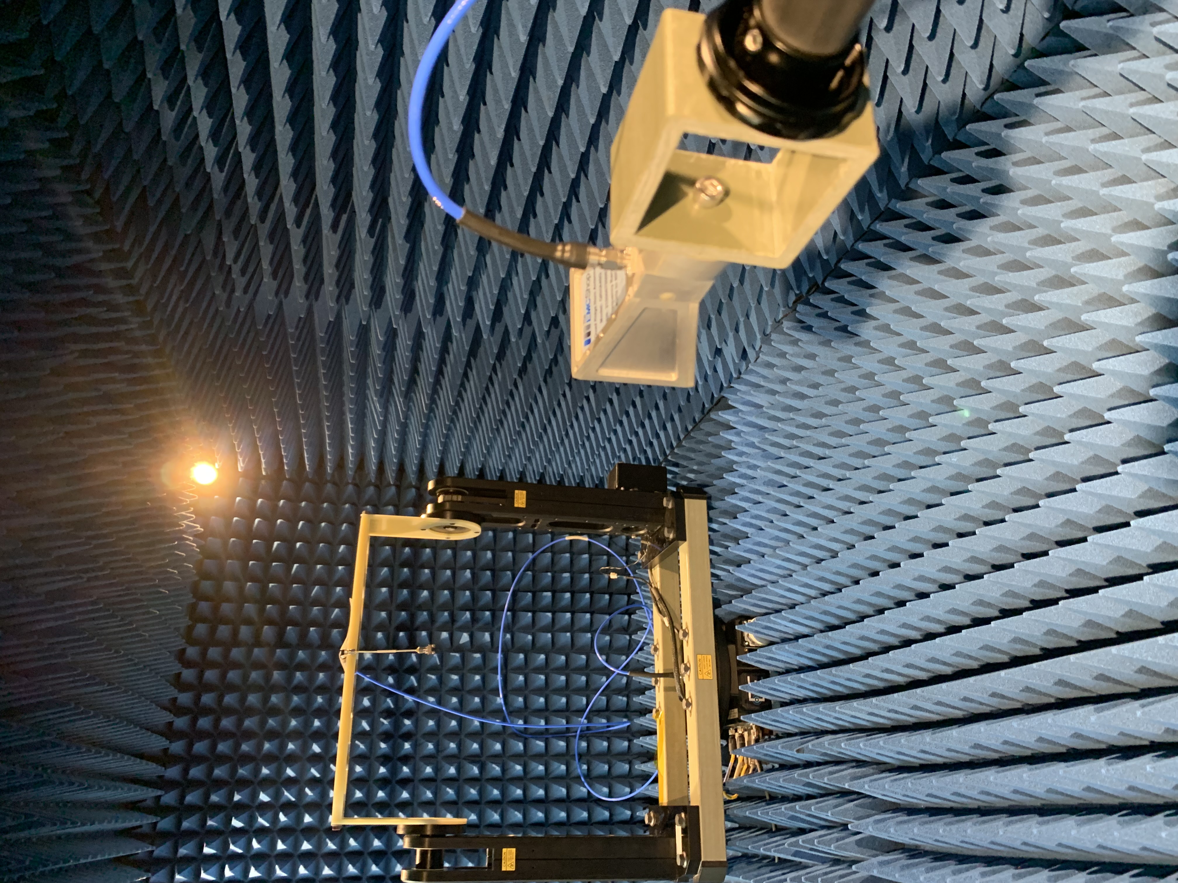
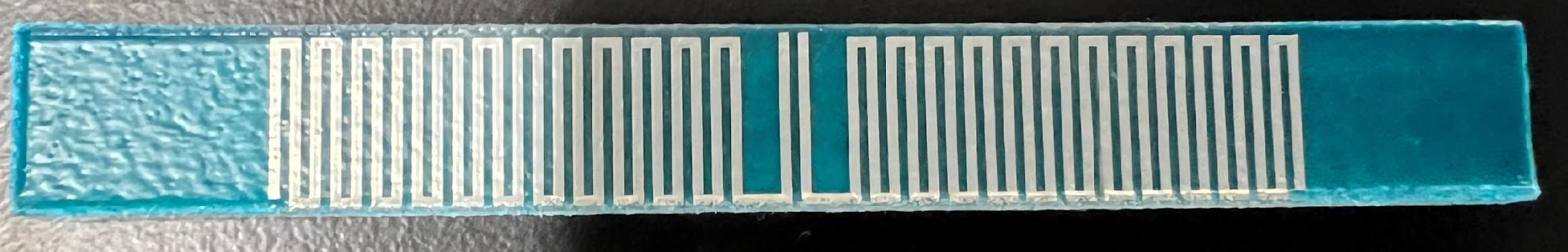
Thin-Film Antennas on Willow Glass and Ribbon Ceramic | Corning Collaboration
Collaborated with Corning Inc. to fabricate and test thin-film antennas on flexible Willow Glass substrates optimized for mmWave bands.
- Developed fabrication processes compatible with ultra-thin flexible glass and ceramic to produce conformal mmWave antennas.
- Measured excellent return loss characteristics at the target 28 GHz and 39 GHz bands, validating antenna performance for 5G/mmWave applications.
- Characterized substrate/mechanical integration and demonstrated the potential of Willow Glass for high-frequency flexible RF modules.
Tech: Willow Glass, thin-film antennas, e-beam evaporation, photolithography, through-glass-vias, RF testing
View details
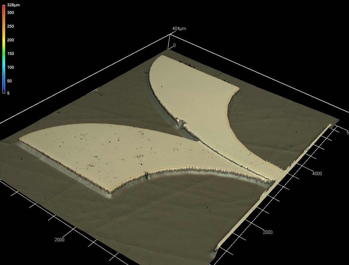
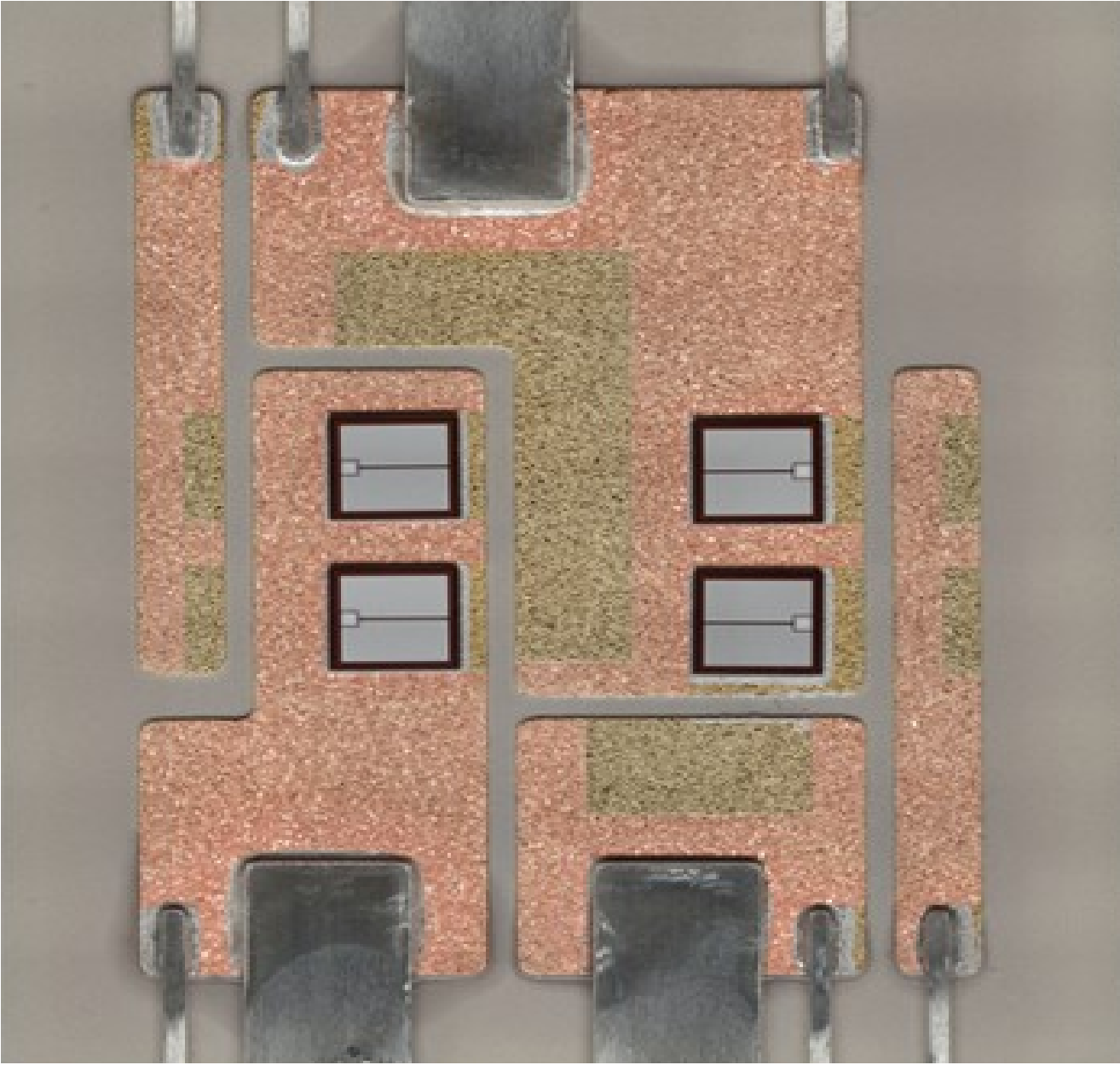
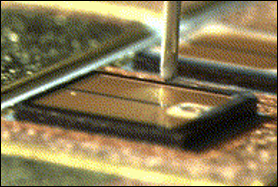
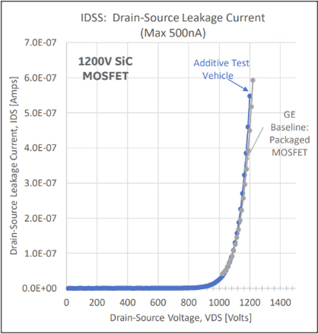
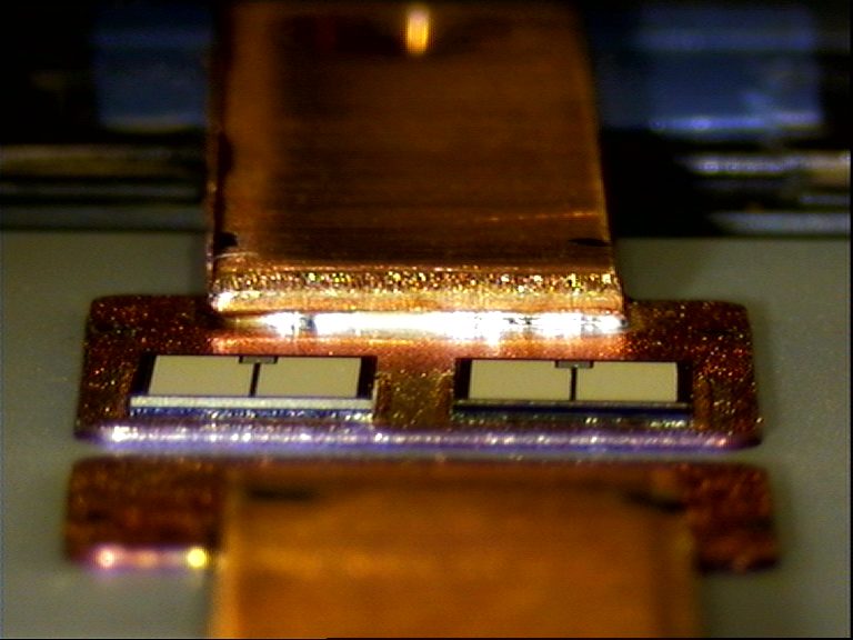
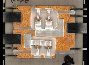
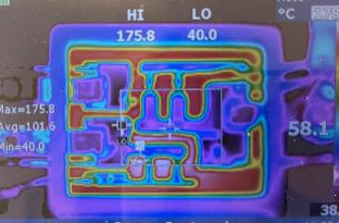
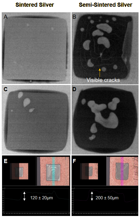
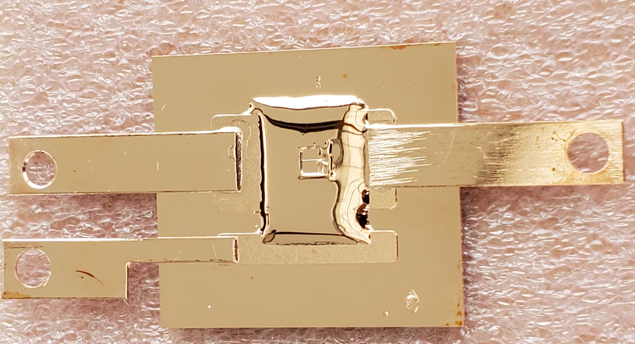
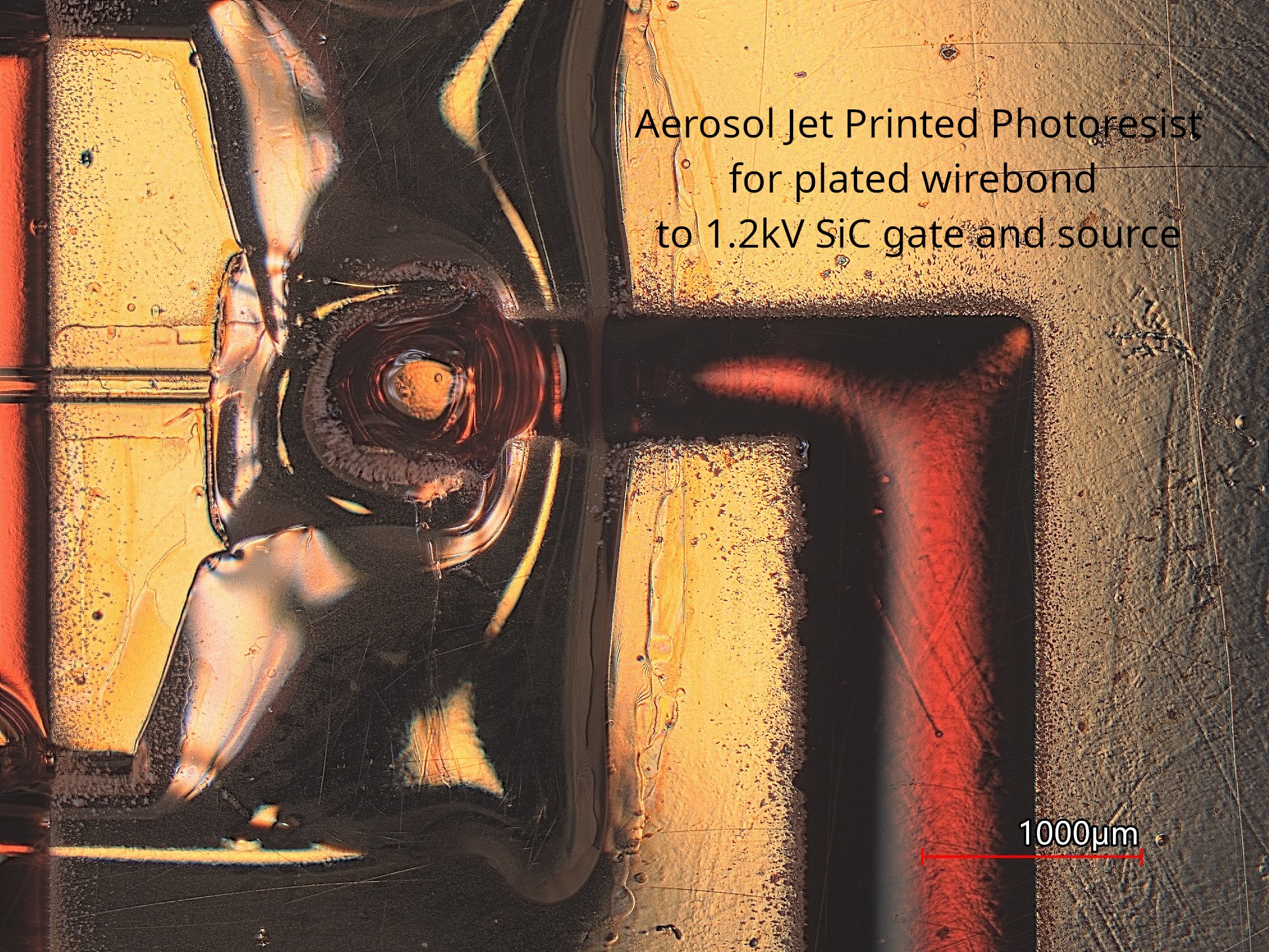
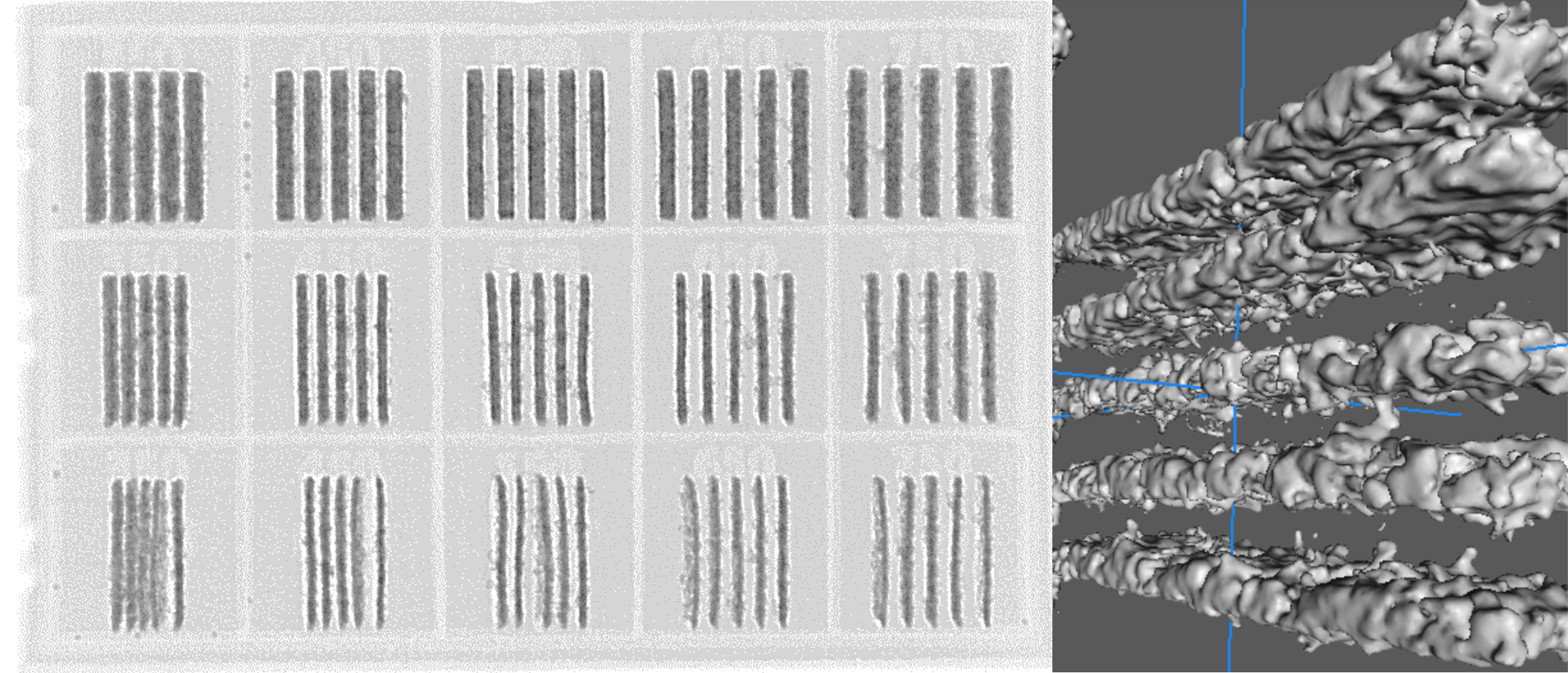
Printed Power Module Packaging & High-Power Applications | GE Collaboration
Developed printed-electronics approaches for power module packaging, including multi-chip SiC power modules and printed interconnects suitable for high current and thermal loads.
- Explored direct ink writing and printed copper for power interconnects and module assembly.
- Published related work in IEEE journals on SiC power module packaging and power-handling performance.
- Demonstrated process improvements that reduce contact resistance and enable scalable printed power solutions.
Tech: Direct ink writing, aerosol jet, printed copper, SiC power modules, thermal testing
View details
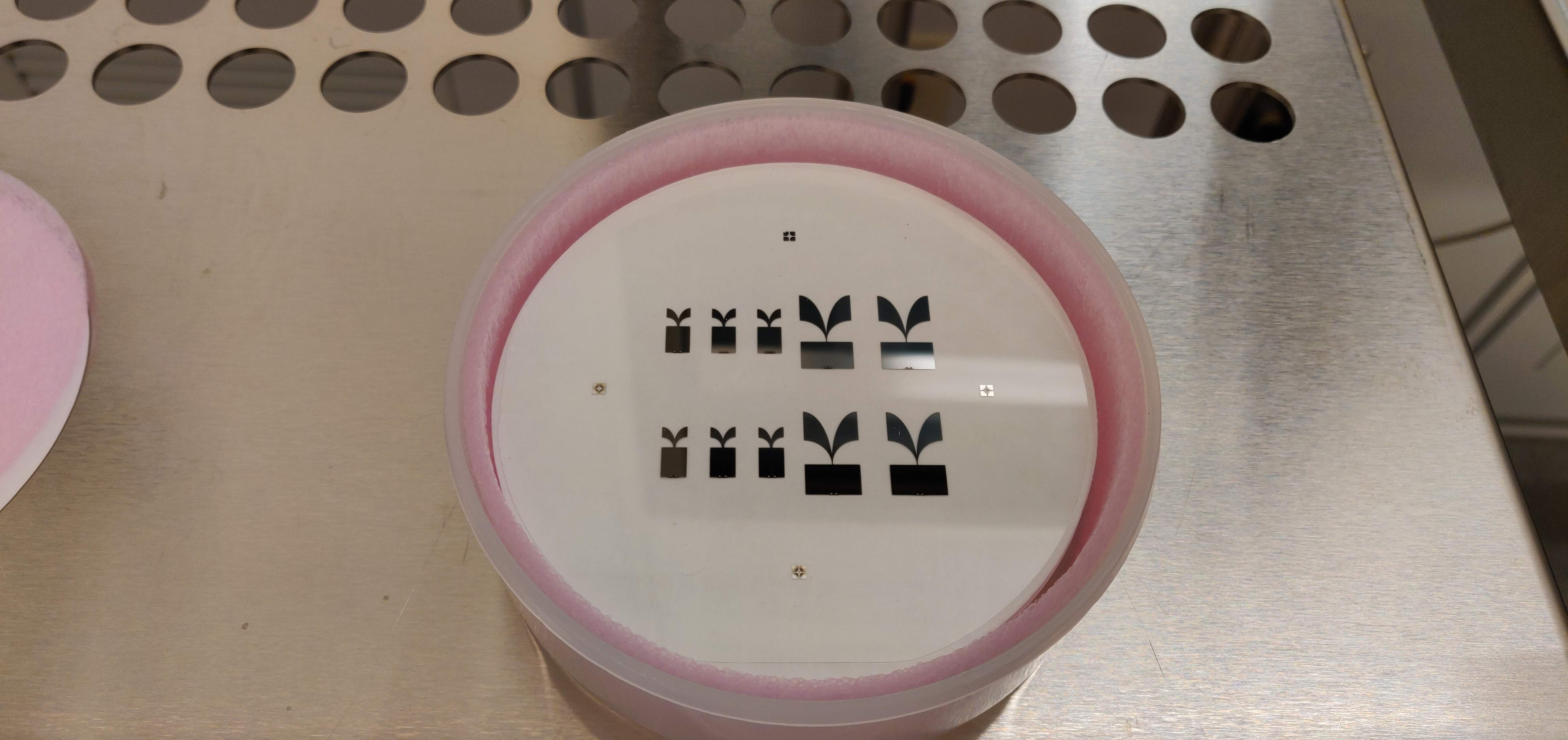
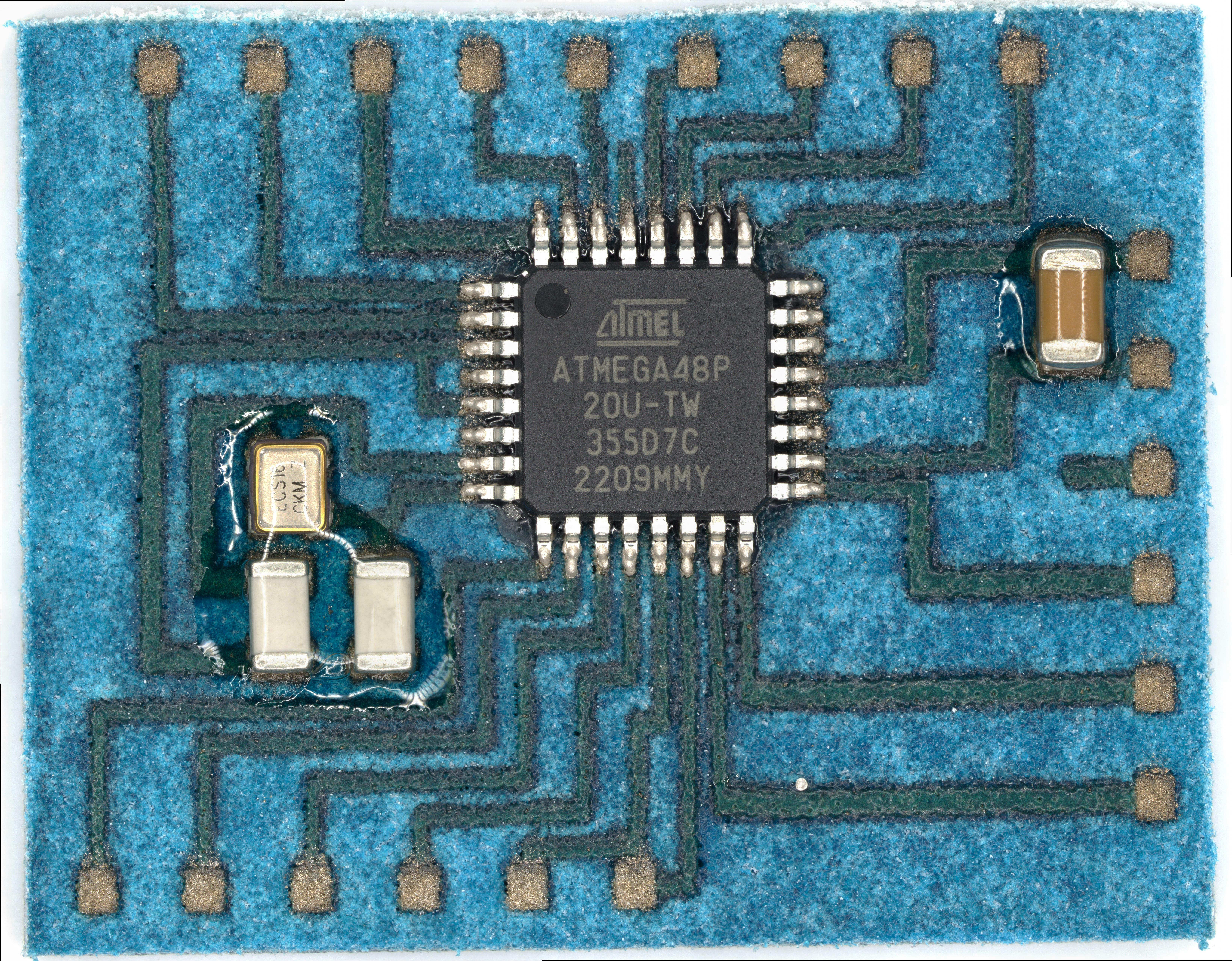
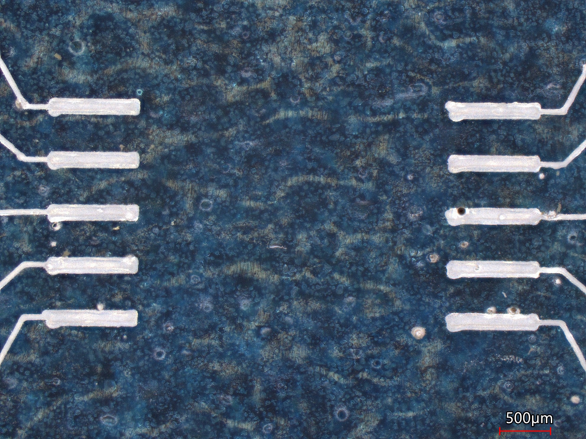
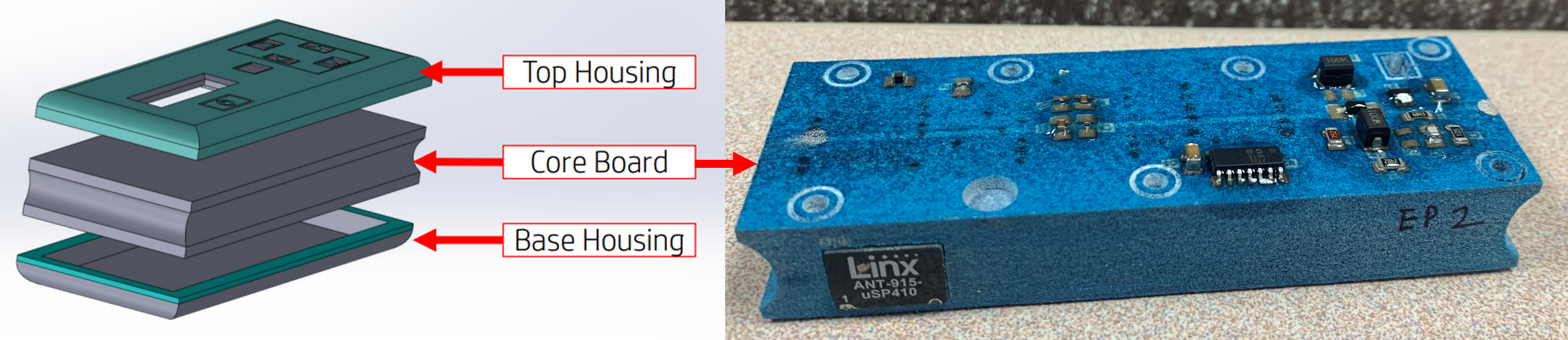
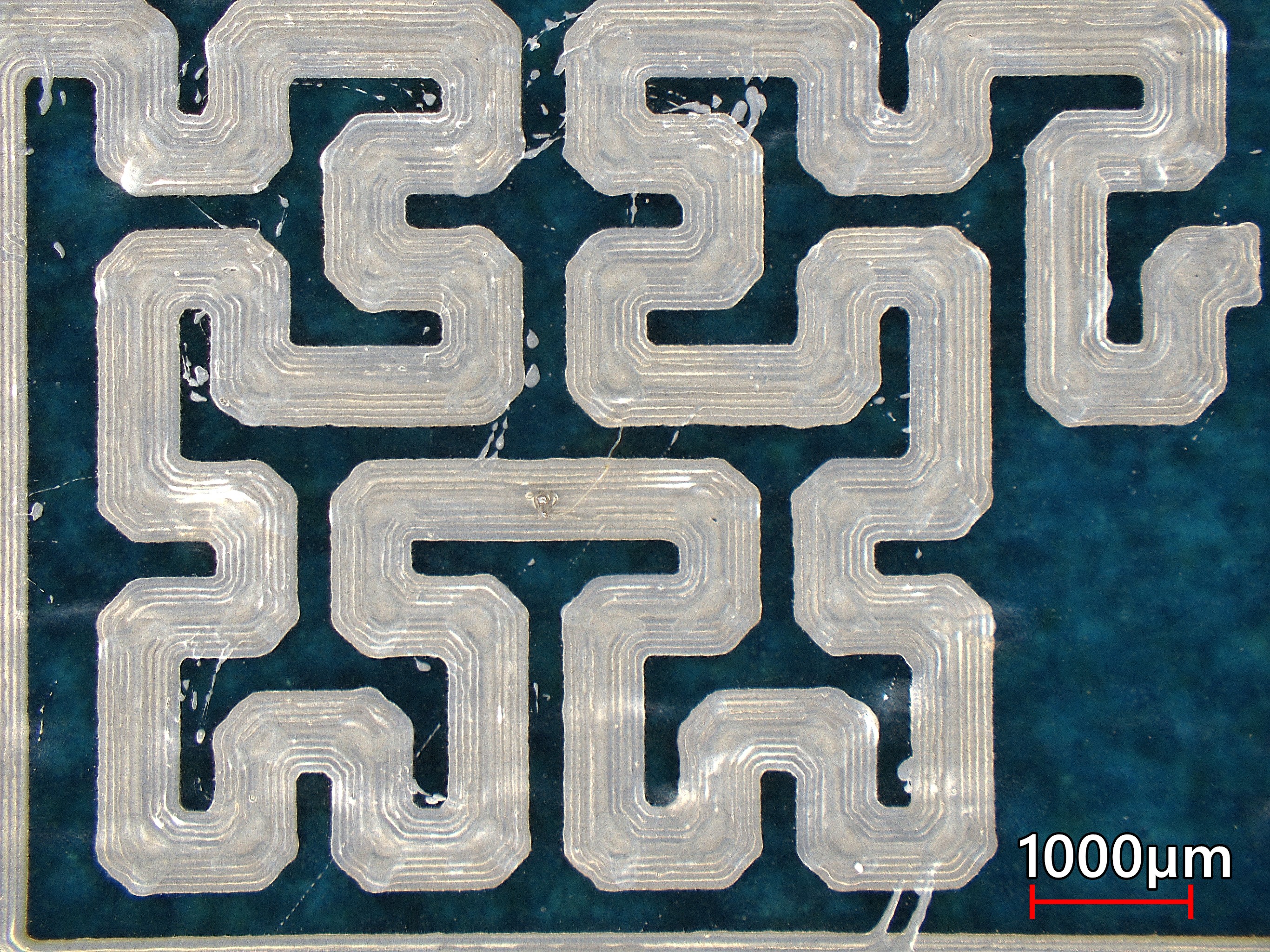
3D Printed Electronics with Multi Jet Fusion | HP collaboration
Collaborated with HP to embed conductive pads, traces, and vias in Multi Jet Fusion 3D-printed parts and integrate aerosol-jet-printed fine-pitch features.
- Demonstrated embedding of electronics within 3D geometry, enabling volumetric interconnects and component placement.
- Improved fine-pitch capabilities by combining MJF with aerosol jet printing to place finer traces and pads.
- Printed RF antennae
Tech: Multi Jet Fusion, aerosol jet printing, embedded vias and wiring, pick-and-place
View details
Flexible Hybrid Electronics Devices & Component Attach Materials
Developed functional FHE devices including RFID/security tag, flexible temperature sensor, and NFC humidity sensor — with comprehensive investigation of silver ink and epoxy interfaces for reliable low-temperature assembly.
- Integrated printed antennas, sensors, and microcontrollers on flexible substrates; demonstrated wireless communication and sensing prototypes at industry events.
- Investigated electrical and mechanical performance of silver nanoparticle inks and silver-filled epoxies through FTIR, SEM, die-shear, current-capacity, and power-cycling experiments.
- Identified failure modes and recommended material/process combinations for improved FHE reliability; evaluated lifetime and environmental robustness for practical deployment.
Tech: Aerosol jet printing, printed antennas, silver inks, conductive epoxies, thermal/power cycling, sensor integration, low-temp die attach
View details